
New ATE Requirements from Advanced Packaging: From Single Chip to System-Level
Advanced packaging has changed what it means to test a semiconductor device. For years, automatic test equipment, or ATE, was optimized around a simple idea: validate one chip, one die, one set of pins, one set of failure modes. That world is fading fast. In its place is a much richer and more complicated one, where the “device” under test may be a multi-die package, a chiplet-based module, a 3D stack, or a heterogeneous system built from several process nodes and several vendors.

This shift from single-chip testing to system-level testing is not a minor adjustment. It changes the entire logic of ATE planning, hardware architecture, software flow, failure analysis, and even business models. In advanced packaging and heterogeneous integration, the package is no longer a passive shell. It is part of the product, and ATE must evolve to treat it that way.
Why the Old Test Model Is Not Enough
Traditional ATE was built for a simpler landscape. The goal was to verify functional correctness, parametric behavior, and reliability of a single die before or after packaging. Test vectors, pin counts, timing budgets, and load boards were all designed around one chip at a time. That model worked well when most integration happened on a single die and the package was just a connection path.
Advanced packaging breaks that model in multiple ways. A modern package may include:
- Multiple chiplets from different process nodes.
- HBM stacks integrated with logic dies.
- 3D connections through hybrid bonding or TSVs.
- Fan-out redistribution layers with dense multi-die routing.
- System-in-package assemblies with analog, RF, power, and digital blocks.
Now the test challenge is not just “does this die work?” but “does this whole integrated system behave correctly under real operating conditions?” That includes interconnect behavior, thermal interactions, power delivery stability, timing across dies, and reliability of the package structure itself. The test problem has become multidisciplinary.
From Die-Level Metrics to System Behavior
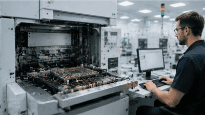
One of the biggest changes in ATE requirements is the shift from die-level metrics to system-level behavior. In a chiplet or 3D package, individual dies may pass independently, yet still fail as a system because the interface between them is faulty or because thermal coupling changes timing and power behavior.
ATE must therefore validate more than core logic. It must also check:
- Die-to-die communication integrity.
- Package-level signal integrity and skew.
- Power distribution across multiple dies.
- Thermal response under load.
- Stack-level fault tolerance and redundancy behavior.
That creates a new class of tests that are part electrical test, part system simulation, and part physical qualification. The package becomes a live part of the device’s behavior, so test strategy must reflect that reality.
Higher Pin Counts and Denser Interfaces
Advanced packaging often means more signals, more power rails, and more test access points. ATE has to cope with increased pin counts and tighter timing margins, especially when chiplets communicate through dense D2D interfaces. Some packages now require test systems that can monitor or stimulate many more interfaces than a traditional single-chip device ever would.
At the same time, many advanced packages hide some of their complexity inside the package itself. That can make direct access harder. The test system must either probe through fewer external pins or rely on built-in test logic and standardized interface protocols. In practice, this drives a stronger need for test compression, scan integration, and embedded diagnostics.
For ATE vendors, this means new hardware front ends, more flexible timing systems, and software capable of handling complicated interface topologies. A tester that once handled one die with a known pin map may now need to manage multiple internal die domains and shared power structures.
Testing Chiplets vs. Testing the Package
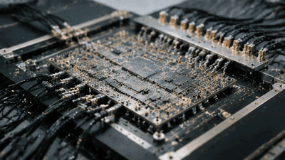
Chiplets introduce one of the most important new ATE requirements: the need to separate chiplet-level testing from package-level testing, then bring them back together at the system level. A chiplet can be good on its own and still fail when assembled into the final package. Conversely, a package can appear to work in a limited test mode but fail under full system load.
This means ATE flows must support multiple test stages:
- Known-good die verification before assembly.
- Intermediate test after partial stacking or bonding.
- Final package test after full assembly.
- System-level test that exercises the package in its real use context.
Each stage has different goals. Early tests screen out defective dies before expensive packaging. Mid-stage tests catch assembly failures or bond issues. Final tests validate the complete package. System-level tests measure whether the device behaves correctly under realistic traffic, power, and thermal loads. Advanced packaging turns testing into a layered process, and ATE must support all layers without becoming a bottleneck.
New Demands on Timing and Synchronization
As interfaces move from board-level to package-level and from single die to multi-die systems, timing becomes much harder to control. D2D links may operate at very high speeds with very tight skew budgets. ATE must therefore provide more accurate timing generation, capture, and synchronization.
This is especially critical for:
- Coherent chiplet systems where latency consistency matters.
- HBM-integrated accelerators with dense parallel interfaces.
- 3D stacks where vertical and lateral signal paths interact.
Even small timing variations can create failures that are difficult to diagnose. A system might pass at one speed bin but fail at another, or behave differently under temperature changes. ATE must be able to isolate those issues and distinguish between a die defect, a package parasitic, and a protocol-level mismatch. That is a much more delicate job than conventional single-chip validation.
Thermal Behavior Becomes a Test Variable
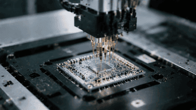
In advanced packaging, thermal effects are not just a reliability concern. They are a test variable. Multiple dies in close proximity generate heat differently, and that heat can affect logic timing, memory stability, and even interface integrity. A device may behave perfectly when cool and fail when heated, or vice versa.
ATE therefore needs better thermal awareness. That can include:
- Temperature-controlled test flows with tighter ramp control.
- Dynamic load patterns that simulate hotspot formation.
- Monitoring of performance drift under thermal stress.
- Validation of thermal throttling or load balancing logic built into the package.
For 3D ICs and tightly packed chiplets, this is especially important because thermal coupling between dies can create cross-effects that are invisible in standard single-chip test. ATE has to help reveal whether the system stays stable when real heat flows through it.
Built-In Test and Design-for-Test Are More Important Than Ever
Advanced packaging makes built-in test, or BIST, and design-for-test, or DfT, much more valuable. The more deeply integrated the package becomes, the harder it is to access every internal connection directly from external ATE. That means more intelligence has to live inside the package itself.
Modern advanced packages increasingly include:
- On-chip test controllers.
- Boundary scan and chiplet-level access mechanisms.
- Built-in self-test for memory, logic, and interconnect.
- Health monitoring for voltage, temperature, and link integrity.
These features help reduce ATE complexity by shifting some test burden inside the system. They also make it possible to perform more meaningful system-level checks. Instead of merely asserting that a pin toggled correctly, the tester can ask whether the whole package responded correctly under a realistic workload.
That is a big difference. It turns ATE from a simple pass/fail gate into a system validation partner.
Yield Learning Needs Better Data
Advanced packaging also changes the economics of yield learning. In a multi-die system, failures can arise from the dies, the bond interface, the interposer, the substrate, the package assembly, or the test flow itself. ATE must provide enough diagnostic resolution to tell these possibilities apart. Otherwise, yield losses become expensive mysteries.
This creates a demand for richer data collection and smarter analysis. ATE systems need to capture more context around every failure, including:
- Test conditions at the time of failure.
- Package and die configuration details.
- Timing, thermal, and voltage corner data.
- Historical behavior across prior test steps.
With that information, manufacturers can begin to understand which failure modes are due to process variation, which are due to assembly issues, and which are due to package architecture. That insight is essential if advanced packaging is going to scale economically.
New Pressure on ATE Economics
From a business standpoint, advanced packaging changes what customers expect from ATE. They need more capable testers, but they also need better cost efficiency because package complexity already raises manufacturing expense. ATE therefore has to deliver more value without simply becoming more expensive in line with package complexity.
This pushes the industry toward several trends:
- More reuse of test content across product families.
- Greater reliance on modular test hardware.
- Higher levels of software automation and analytics.
- Test strategies that reduce unnecessary over-testing while preserving coverage.
In advanced packaging, over-testing can be as damaging as under-testing. If ATE time becomes too long, it can erode the economics of the entire package. That means the new ATE requirement is not just technical sophistication. It is intelligent efficiency.
System-Level Test Requires System Thinking
The most important shift may be cultural. Advanced packaging forces test engineers to think like system engineers. That means looking beyond one chip, one interface, or one failure mode. It means understanding how dies interact, how the package changes behavior, and how real workloads affect reliability and performance.
This broader view is especially necessary for chiplets. A chiplet system might include CPU logic, AI acceleration, memory, security, and I/O all in one package. The tester must not only confirm that each block works but that the interactions between blocks work as intended. That is a more demanding form of validation, and it blurs the line between production test and full system bring-up.
As a result, test teams increasingly need cross-functional collaboration with architecture, packaging, thermal, and reliability engineers. ATE no longer sits at the end of the flow. It participates in design decisions much earlier.
Where ATE Is Heading
The future of ATE in advanced packaging will likely be defined by three things: more system awareness, more built-in intelligence, and more flexibility. Testers will need to support many package types, many interconnect styles, and many levels of access. At the same time, they will need to provide richer data with faster decision-making.
We can expect to see:
- More package-aware test planning.
- Greater use of embedded diagnostics and in-package observability.
- Smarter correlation between wafer test, package test, and system test.
- Closer integration between ATE data and yield analytics.
In other words, ATE is evolving from a single-chip validator into a system-level intelligence platform. That may sound ambitious, but it is exactly what advanced packaging demands.
Conclusion
Advanced packaging and heterogeneous integration have fundamentally changed the requirements for automatic test equipment. What used to be a single-chip, single-die world has become a layered system world, where the package itself contributes meaningfully to performance, reliability, and failure behavior. ATE must now test chips as systems, not as isolated parts.
That means more timing precision, more thermal awareness, better DfT and BIST support, richer data capture, and stronger system-level thinking. It also means the ATE industry must keep iterating just as fast as the packaging industry does. The companies that get this right will not just sell testers. They will help define how the next generation of multi-die, chiplet-based semiconductor systems are brought to life.





